Micro-Epsilon IMS5420 – White light interferometer for thickness measurement of silicon wafer
The Micro-Epsilon IMS5420 is a state-of-the-art white light interferometer designed for the non-contact thickness measurement of monocrystalline silicon wafers. It is a compact system which is suitable for measurement applications in area where space is restricted or limited. Featuring a broadband superluminescent diode (SLED) with a 1,100 nm wavelength range, it is adept at measuring undoped, doped, and highly doped SI wafers with unparalleled precision.
Key Features:
- Nanometer-Accurate Measurement: Ensures precision in measuring undoped, doped, and highly doped wafers.
- Multi-Layer Detection: Capable of acquiring up to 5 layers with a silicon thickness range of 0.05 to 1.05 mm.
- High Resolution: Offers a high z-axis resolution of 1 nm.
- Fast Measurement: Achieves a measuring rate of up to 6 kHz.
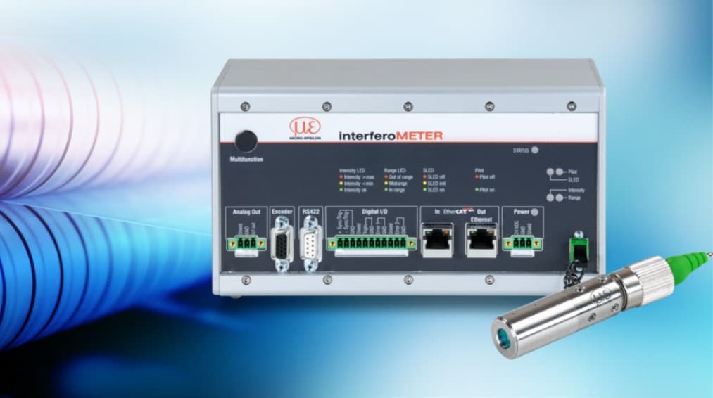
- Versatile Connectivity: Supports Ethernet, EtherCAT, RS422, PROFINET, and EtherNet/IP.
- User-Friendly Interface: Allows easy parameterization via a web interface.
Integration and Interfaces
Controller Interfaces: Integrated interfaces like Ethernet, EtherCAT, RS422, additional encoder connections, analog outputs, synchronization inputs, and digital I/Os.
Additional Integration: Using Micro-Epsilon's interface modules, PROFINET and EthernetIP compatibility is provided, enabling integration into various control systems and production programs.
Measuring Range:
For Silicon: 0.05 to 1.05 mm
For Air Gap: 0.2 to 4 mm
Accuracy: Less than ±100 nm for single layer measurement.
Distance: Effective from approximately 24 mm with a working range of about 6 mm.
Applications:
Wafer Thickness Measurement: Ideal for monocrystalline silicon wafers with a geometric thickness of 500 to 1050 µm, and a doping of up to 6 m Ω cm.
Inline Measurement: Used in lapping and grinding machines for inline thickness measurement to ensure high process stability and quality control.
Enquire Now